PIO Breakout
In order to properly develop and debug a piece of hardware on the PIO port, a breakout board can quickly become a very useful resource.
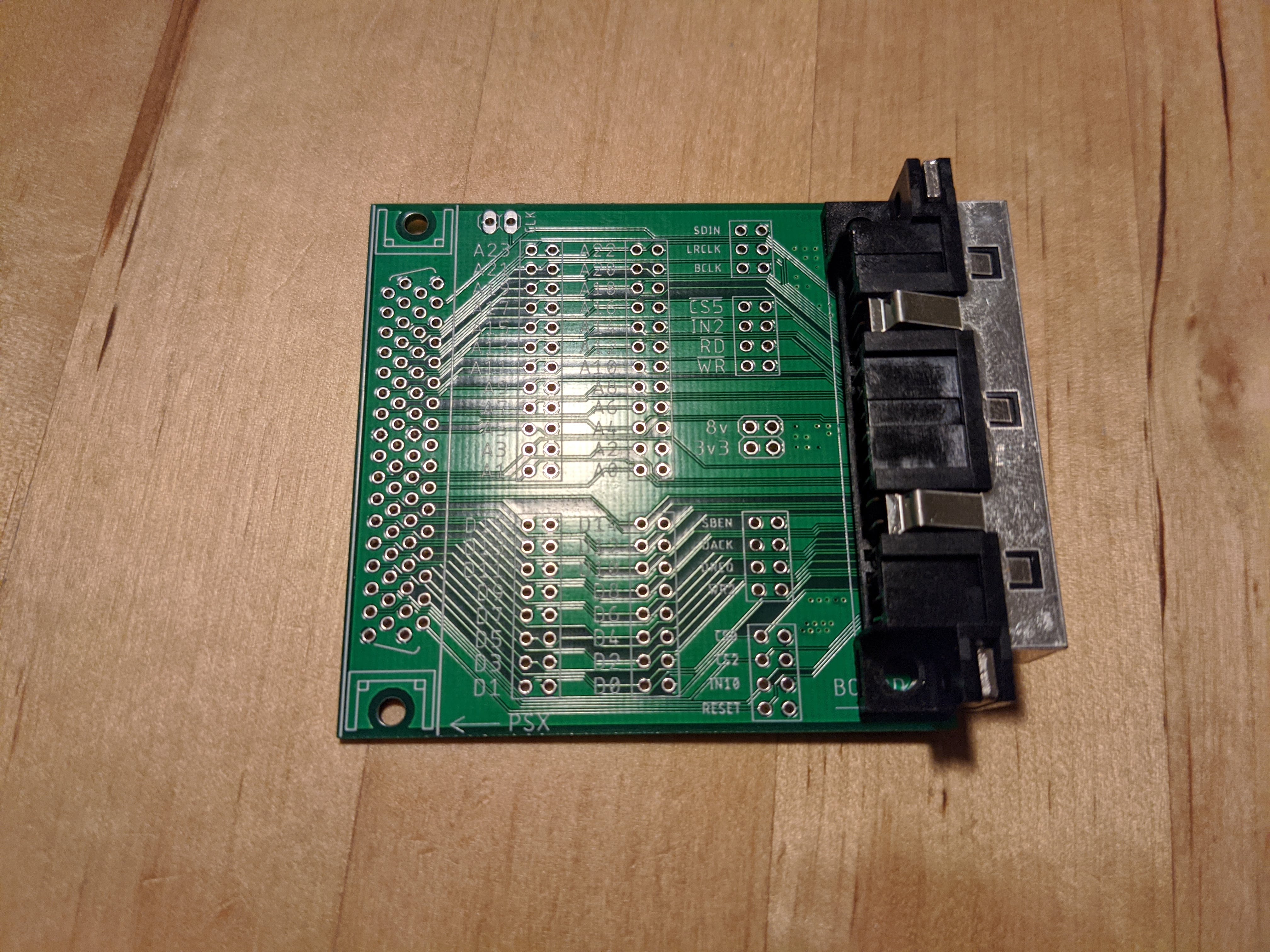
The breakout board design files are committed into the repository, and are available through oskpark too.
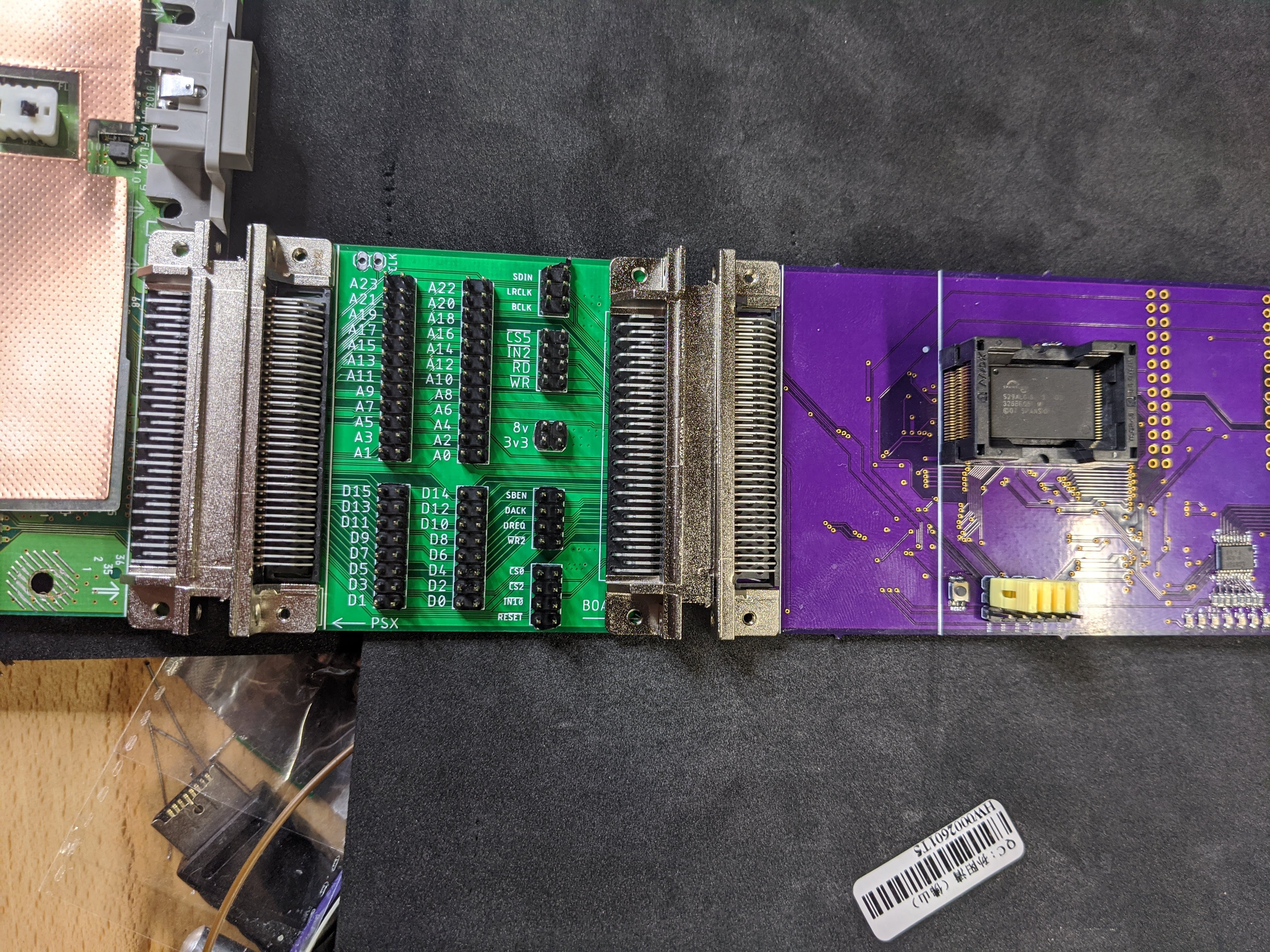
It is designed to act as a pass-through, with the same footprint as the genuine PIO connectors, provided that it is populated with the appropriate plugs. See the replacement connector page for some details about this.
If the motherboard plug is removed to install one of the suggested plugs above, then the breakout board can be fitted with it, in order to provide an adapter board to plug genuine cheat carts.
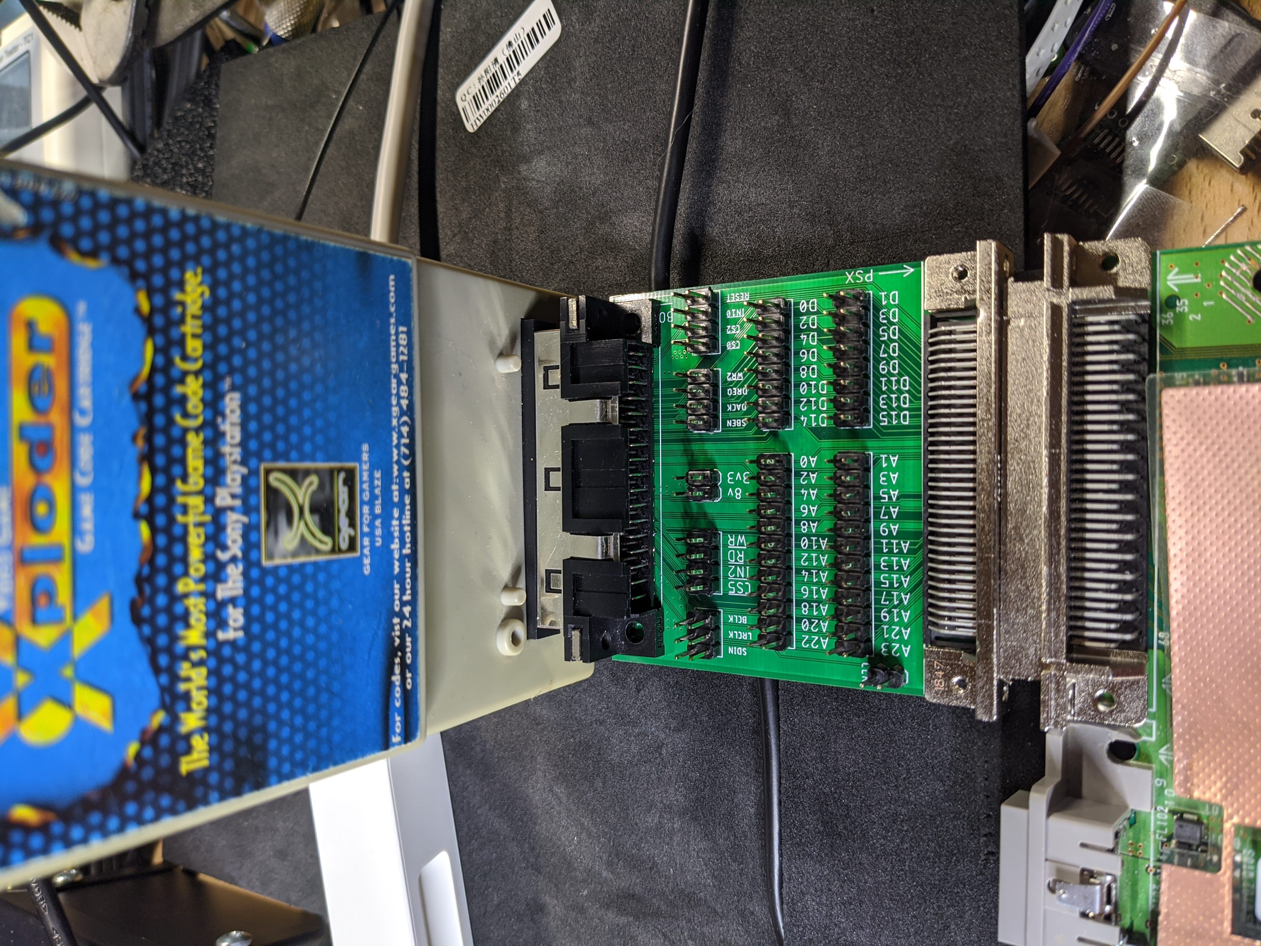
It of course can still be fitted with replacement connectors to work on modern carts:

The silkscreen is describing the pinout on both sides of the board, allowing for a horizontal or vertical connection. The pin number of each pin is also drawn, although this could be hidden by the solder flux when the connector is populated.
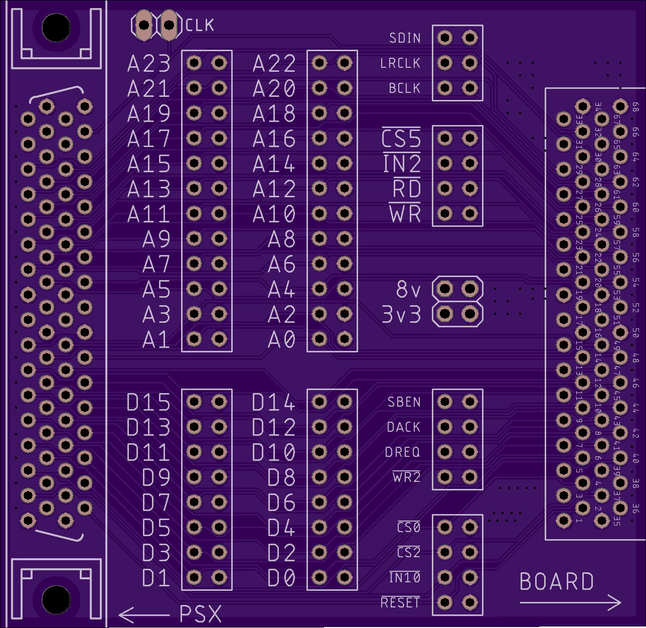
The signification of each signal is better described in the main PIO page. Each connector is paired with a ground, and both layers of the PCB are flooded with ground planes.
The ground pin is always the one without a label, which means that on the picture above, the ground pin is always on the right side, except for the CLK signal, for which it sits on the left.
The Digilent Digital Discovery USB logic analyzer has been found to work well with this breakout board, with enough channels and memory to deal with most of the required debugging workload for this tool.
Although it shouldn't matter with the speed at which the PlayStation's CPU is operating, the reader is advised that no effort has been made to match length on the PCB traces, which could cause signal skewing.